

![]()
BASIC
METAL OXIDE SEMICONDUCTOR FIELD EFFECT TRANSISTOR: SCIENTIFIC ASPECTS
click here to learn more about the development of this
transistor
The MOSFET may be considered as a much-advanced upgrade of the JFET. It has shown great promise of achieving wide commercial acceptance and is the most commonly used transistor in the highly complex electronic devices. However, MOSFET too is present in different types. We shall, for the sake of simplicity, consider the Depletion-Enhancement or simply DE-MOSFET, which is the modified version of MOSFET and is the most suitable one.
Construction:

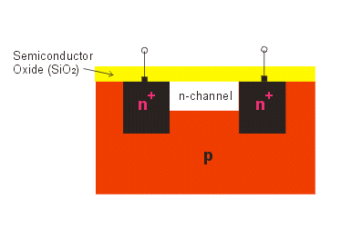
Consider a MOSFET shown in the adjoining diagram. It consists of a p-type semiconductor (shown in red) with two n-regions (shown in black) that are embedded into it by special techniques. These n-regions contain extremely high number of charge-carriers (electrons) and so are represented as n+. This combination is then covered over by a layer of the semiconductor's oxide. In between the two n+ regions, is another channel of n-type semiconductor (shown in white), containing less number of charge carriers than the n+ regions.
Working:
 When a
negative charge is applied above the layer of oxide, the n-channel attracts most available
positive charges (holes) towards itself (since opposite charges attract). Thus the flow of
electric current, which is actually the flow of negatively charged electrons is reduced
due to the presence of the opposite positive charge. This is called as Depletion of
current.

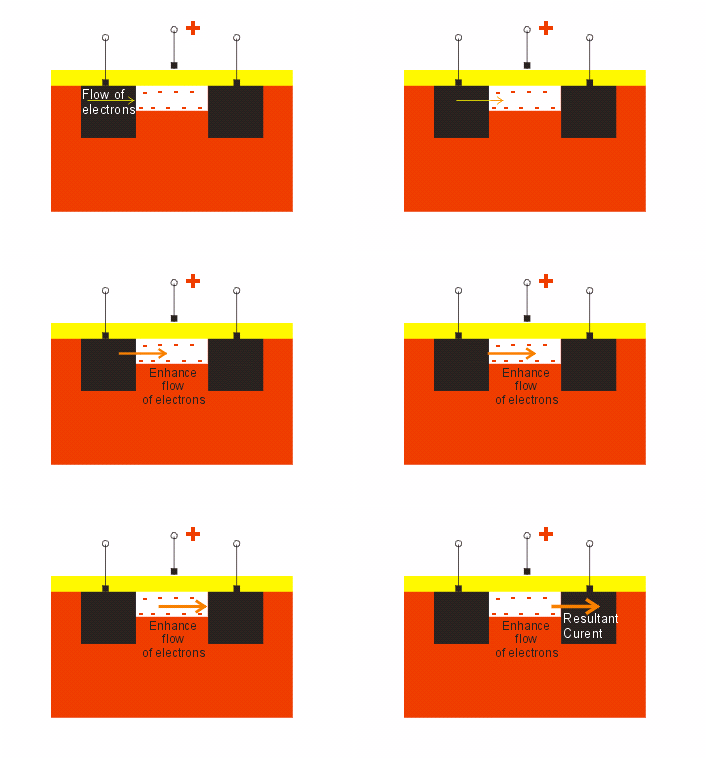
On the other hand, when a positive charge is applied above the layer of oxide, the n-channel attracts more electrons towards itself. Thus the flow of current, which is nothing but the flow of electrons, is enhanced by these surplus electrons.
Hence the name, Depletion-Enhancement MOSFET.
Here, the n+ region from where the electron current enters is called as the Source. The other n+ region from where they leave is the Drain. The charge above the oxide layer is called as Gate. Thus, just as in case of a tap, the flow fom the Source to the Drain is controlled by the Gate.
The same explanations are valid for p-channel MOSFET. However, the electrons will be replaced by holes and vice versa, and the charges will be reversed.