

![]()
ADVANCED
METAL OXIDE SEMICONDUCTOR FIELD EFFECT TRANSISTOR: SCIENTIFIC ASPECTS
click here to learn more about the development of this
transistor
T he MOSFET may be considered as a much-advanced upgrade
of the JFET. It has shown great promise of achieving wide commercial acceptance and is
the most commonly used transistor in the highly complex electronic devices. However,
MOSFET too is present in different types. We shall, for the sake of simplicity, consider
the Depletion-Enhancement or simply DE-MOSFET, which is the modified version
of MOSFET and is the most suitable one.
Construction:

Let us consider an n-channel DE-MOSFET. It consists of a lightly doped p-substrate into
which are etched two highly doped n-regions. These two regions are so highly doped that
they are represented as n+. The oxide of the semiconductor (e.g. SiO2) then
layers this combination. The two n
Working:
The voltage that is to be amplified is applied between the Drain and the Source and is
called as the Drain-Source voltage (V
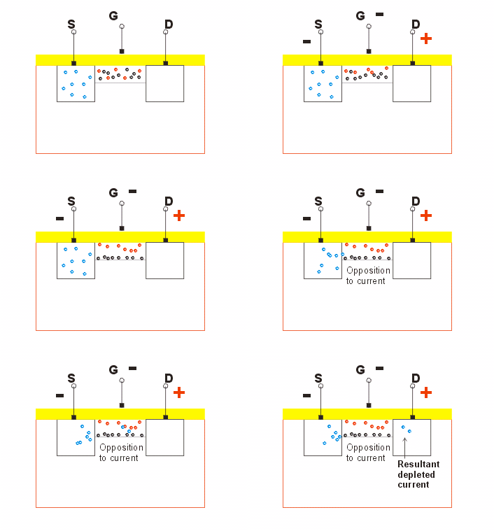
 When VGS is made negative,
the gate terminal G acquires a negative potential. Consequently, there occurs an induction
of charges through the semiconductor oxide, as shown. As a result, the positive charges
that are present in the n-channel get concentrated towards the gate terminal, thus
reducing the flow of electrons from the Source to the Drain. This reduction of electric
current is called as Depletion.
 Converse effect is observed when VGS
is made positive. The gate terminal G now acquires a positive potential. Once again, an
inductive effect is observed and this time, the negative charges that are available are
concentrated towards the oxide layer. Thus, they help in facilitating the flow of current
between the Source and Drain. This effect is called Enhancement.
Thus the oxide layer prevents the direct contact between the gate and the n-channel, thus preventing the flow of current between them. Also, the n-channel plays an important role by providing adequate positive and negative charges during induction.
The same explanation is valid for p-channel MOSFET. But the regions, charges and the voltages will have to be reversed.