


![]()
![]()
![]()
BASIC
JUNCTION FIELD EFFECT TRANSISTOR: SCIENTIFIC ASPECTS
click here to learn more about the development of this
transistor
 C
onstruction:
C
onstruction:
The construction of a JFET can best be considered by studying the adjoining diagram. It looks like a black channel passing between two red bodies, which is exactly what it is. A channel of n-type semiconductor is contains two p-type blocks on its either side. Such a JFET is called as the n-channel JFET.
Replacing the n-region by p-region and vice versa leads to a p-channel JFET
Working:
Let us discuss the working of an n-channel JFET.
 In a working transistor, the current
that is to be amplified is flows through the channel (shown in black). A separate voltage
is applied to the p-regions (shown in red).
In a working transistor, the current
that is to be amplified is flows through the channel (shown in black). A separate voltage
is applied to the p-regions (shown in red).
In such an arrangement, there will be an electric field due to the voltage applied to p-regions. And just as you might have seen two magnets affecting each other, in the same way, the electric current is affected by the presence of electric field on these p-regions. If the electric field is decreased, the current in the channel increases and if the electric field is increased, the current decreases. Thus by effect of the electric field the current is controlled. Hence the name Field Effect Transistor
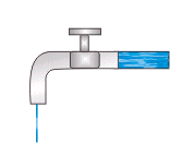 A point of interest here is to note that this functioning is analogous to
the working of a tap. The water enters the tap through a Source, its flow is controlled by
means of a Gate and the resultant flow is the Drain.
A point of interest here is to note that this functioning is analogous to
the working of a tap. The water enters the tap through a Source, its flow is controlled by
means of a Gate and the resultant flow is the Drain.
Similarly, the part of the transistor where the electrons enter is the Source. The
p-regions whose field controls the current are called as Gate. And the other end of
the channel where the electrons leave is the Drain.
The same explanation will hold valid for p-channel JFET.