


![]()
![]()
![]()
ADVANCED
JUNCTION FIELD EFFECT TRANSISTOR: SCIENTIFIC ASPECTS
click here to learn more about the development of this
transistor
C onstruction:
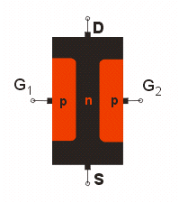
Consider an n-channel JFET that is illustrated in the adjoining figure. A semiconductor body is doped lightly with an n-type impurity to form an n-channel. Its two ends are connected to two terminals called the Drain (D) and Source (S) respectively. On either side of the channel are deposited much heavily doped p-type regions. These are connected to separate terminals called Gate terminals (G1 and G2) and are wired together in use. These p- and n-regions are interchanged to obtain a p-channel JFET.
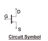
Working:
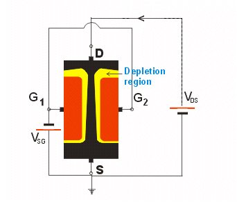
Consider the n-channel JFET connected in a standard circuit as shown. As is evident, the electrons will enter the channel from the Source (S) terminal and leave from the Drain (D) terminal. Also both the p-n junctions are reverse biased.
Due to this reverse biasing, there will be an increase in the depletion region in the n-channel. As the n-region is lightly doped in relation to the p-region, most of the depletion region will spread into the n-channel than into the p-region. Also the potential due to the voltage applied to the D and S terminals (the Drain-Source voltage - VDS) is larger towards the S terminal, the resistance offered to the current flow near S terminal is less. So the depletion region is narrower towards the S terminal and larger toward the D-terminal.
This depletion region effectively controls the current flow. As the Source-Gate (VSG) voltage is increased, the depletion region increases and so the current flow is decreased. On the other hand, a decrease in VSG increases the current flow.
This explanation will hold equally valid for p-channel JFET. However, the electrons
will be replaced by holes and the voltage will be reversed.