


![]()
![]()
![]()
POINT CONTACT TRANSISTOR:
SCIENTIFIC ASPECTS
click here to learn more about the development of this
transistor
T his is the first transistor that was built. While it seems quite primitive considering today's magnificent circuits, it in fact laid the foundations for the development of a transistorized world.
Construction:
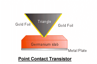 This transistor consists of a slab of germanium semiconductor placed on the
top of a metal plate. This semiconductor is n-type (that is with excess electrons). On the
top it is placed a triangle which is covered with a gold foil and the tip of the triangle
is then cut to create an extremely small gap between the two gold contacts - measuring
almost 0.002 inches. While this distance is easily achievable by machines today, it
was difficult to achieve the same almost 50 years ago! (To cut it short, today's machines
that can create a width of .002 inches are invariably operated by transistors. Then
certainly, to obtain the first transistor, you need some other technique!)
This transistor consists of a slab of germanium semiconductor placed on the
top of a metal plate. This semiconductor is n-type (that is with excess electrons). On the
top it is placed a triangle which is covered with a gold foil and the tip of the triangle
is then cut to create an extremely small gap between the two gold contacts - measuring
almost 0.002 inches. While this distance is easily achievable by machines today, it
was difficult to achieve the same almost 50 years ago! (To cut it short, today's machines
that can create a width of .002 inches are invariably operated by transistors. Then
certainly, to obtain the first transistor, you need some other technique!)
This triangle with its gold foil is then inverted and placed on the germanium semiconductor so that it lightly touches the slab.
Working:
The working of this transistor differs from the other types of transistor. To put its principle in one sentence, the current that is to be amplified alters a much larger current and makes the latter mimic itself.
Here is how the process of amplification occurs.
When a current is applied to one of the contacts, electron-deficient spaces, called as holes, are created in the N-type (negative) semiconductor. This amount of holes that are fed into the N-type semiconductor forms a layer of P-type (positive) semiconductor at the surface. The boundary between N- and P-type semiconductor is known as a PN junction. When a PN junction is formed, it allows for current to flow from one side of a semiconductor, to the other. Therefore, when this junction is formed, the metal plate, which is attached to a high voltage source, transmits a large current through the semiconductor to the second contact, where it exits. This happens because until holes were injected into the semiconductor, there was no PN junction, therefore it did not allow current to flow properly through it. When it was created, it allowed for the external high voltage to flow through it, mimicking it and thus amplifying it.
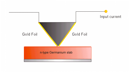
If you've really been following, you may be wondering how the second high voltage current actually mimics and then amplifies the small weak current that was fed into the first contact. Well, think about it this way: First of all, semiconductors are very well suited to do this job, because they are extremely sensitive. Every time a signal/current is fed into the first contact, it injects more holes into the semiconductor. This signal can vary, for example if it is a voice, or a song, it can get larger and smaller (in terms of a voice, by getting larger and smaller, it would mean speaking louder or softer, or at different tones). But as it gets larger and smaller, so does the PN junction. Logically, if the PN junction is smaller, then a smaller percentage of the other, high voltage can flow through the semiconductor. This can work the other way, too. If the PN junction is larger, then a higher percentage of the external, high-voltage current can flow through the semiconductor. In this way, as the signal gets larger and smaller, so does the current attached to the metal plate, thus mimicking it, but at a higher voltage. This is called amplification.
This was probably the earliest process of amplification, carried out by the first transistor ever. However, due to much advanced principles that were employed by the future transistors, it finally faded into the background…