

Scientific Aspects
Click to learn about the development of this transistor
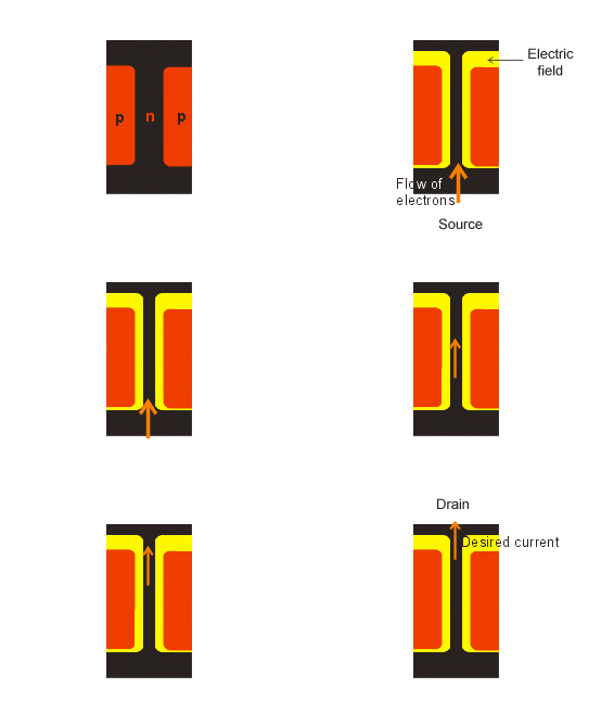
The construction of a JFET can best be considered by studying the adjoining diagram. It looks like a black channel passing between two red bodies, which is exactly what it is. A channel of n-type semiconductor is contains two p-type blocks on its either side. Such a JFET is called as the n-channel JFET.
Replacing the n-region by p-region and vice versa leads to a p-channel JFET
Working:
Let us discuss the working of an n-channel JFET.
In a working transistor, the current that is to be amplified is flows through the channel (shown in black). A separate voltage is applied to the p-regions (shown in red).
In such an arrangement, there will be an electric field due to the voltage applied to p-regions. And just as you might have seen two magnets affecting each other, in the same way, the electric current is affected by the presence of electric field on these p-regions. If the electric field is decreased, the current in the channel increases and if the electric field is increased, the current decreases. Thus by effect of the electric field the current is controlled. Hence the name Field Effect Transistor
The same explanation will hold valid for p-channel JFET.
 C
onstruction:
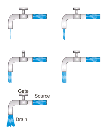 A point of interest here is to note that this functioning is analogous to the working of a tap. The water enters the tap through a Source, its flow is controlled by means of a Gate and the resultant flow is the Drain.
Similarly, the part of the transistor where the electrons enter is the Source. The p-regions whose field controls the current are called as Gate. And the other end of the channel where the electrons leave is the Drain.
|
Development-Scientific |
Development-Scientific |
|
Development-Scientific |
Development-Scientific |
C
onstruction:
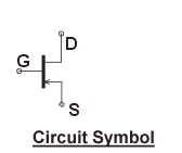
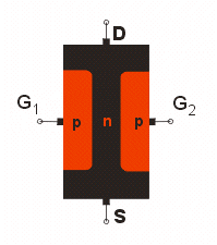
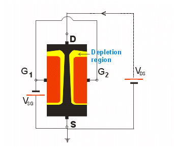
Consider an n-channel JFET that is illustrated in the adjoining figure. A semiconductor body is doped lightly with an n-type impurity to form an n-channel. Its two ends are connected to two terminals called the Drain (D) and Source (S) respectively. On either side of the channel are deposited much heavily doped p-type regions. These are connected to separate terminals called Gate terminals (G1 and G2) and are wired together in use. These p- and n-regions are interchanged to obtain a p-channel JFET.
Working:
Consider the n-channel JFET connected in a standard circuit as shown. As is evident, the electrons will enter the channel from the Source (S) terminal and leave from the Drain (D) terminal. Also both the p-n junctions are reverse biased.
Due to this reverse biasing, there will be an increase in the depletion region in the n-channel. As the n-region is lightly doped in relation to the p-region, most of the depletion region will spread into the n-channel than into the p-region. Also the potential due to the voltage applied to the D and S terminals (the Drain-Source voltage - VDS) is larger towards the S terminal, the resistance offered to the current flow near S terminal is less. So the depletion region is narrower towards the S terminal and larger toward the D-terminal.
This depletion region effectively controls the current flow. As the Source-Gate (VSG) voltage is increased, the depletion region increases and so the current flow is decreased. On the other hand, a decrease in VSG increases the current flow.
This explanation will hold equally valid for p-channel JFET. However, the electrons will be replaced by holes and the voltage will be reversed.
|
Development-Scientific |
Development-Scientific |
|
Development-Scientific |
Development-Scientific |
|
Introduction to Semiconductors
This topic will introduce you to the concept of semiconductors which are an integral part in the making of transistors. |
|
Semiconductor Diodes
The prerequisite information on diodes that later went on to give the birth to the semiconductor triode - otherwise known as the transistor. |
|
Semiconductor Triodes
Another name for the transistor... |
|
Types of Transistors
Learn the various types of transistors and how they function. |
|
Amplification
This is the basic function of the transistor - and the most important one! |
|
Switches
Next to amplification, this is the most common function of transistors. |
|
Comparisions
Learn the analogies and the differences between the older vacuum tube triodes and the slicker new transistors. |
|
Integrated circuits
These are the most common applications of transistors and go a long way in building powerful microprocessors and appliances. Learn the role that transistors play in them. |
|
Microprocessors
These are the real brains of most electronic appliances around us. Explore the vital role played by their grey cells - transistors. |
|
Appliances affected
Realize the full potential of these transistors through the various appliances they revolutionized, right from your digital watch to this PC. |
|
The pre- and post-transistor world
To understand the impact of the transistor in its entirety, perceive what the world was before, and what it is after 1947 - when the transistor was invented. |
|
Future trends
Revolution is an unending process. Take a sneak preview of where the transistors of the future are headed. |
|
History
Understanding of the transistor becomes clearer when learnt in context of its evolutionary journey. Here, we have presented the most important landmarks in its journey of almost a century. |
|
Build the transistor
Theoretical knowledge weighs nothing unless put to practice. Learn how the different types of transistors are built and build some on your own! |
|
Learn the circuits
Learn how the actual amplification and switching takes place by building your own circuits and watching the current flow. |
|
Drive-the-circuit
If you have the necessary stuff in your head, come and test drive a BJT amplification circuit! But watch out for the speed bumps along the way! |
|
Message Boards
Leave your own messages and discuss different topics with fellow surfers. |
|
Ask-a-mentor
Nobody's perfect...we are no exception. But we certainly try to be perfect. If you have any questions about transistors that were not answered in this site, ask our mentors... |
|
Related links
Related links on the web about transistors. |
|
Learners' Center
Discuss your views with other users of this site. There are topics like Message Board, Translate-the-site and Simplify-the-site! |
|
Quizzes
These are quizzes to rack your grey cells. If you think that you have surfed this site entirely, solve these! They include Multiple choice questions and Scrambled words to solve! |
|
Learn in a Flash
These are our step-by-step interactive tutorials to brief you up about the world of transistors. |
|
Advanced Section
This section includes an in-detail explanation on this topic. For you to understand the Advanced section, you should have a basic knowledge of the fundamentals involved. To learn more, please select the section called Prerequisites from the bottom of the page. |
|
Basic Section
Return to the Basic section. |
|
Prerequisites
This section is meant to explain the fundamentals involved in the knowledgae of transistors! This page opens in new window |
|
Site Map
This page will show the map of ...trailing the Transistor for your easier navigation. |
|
Citations and Copyrights
A list of our sources and also copyright notices of material used in making this site. This page opens in new window |
|
Development of PCT
Learn the development of Point Contact Transistor. |
|
Development of BJT
Learn the development of Bipolar Junction Transistor Transistor. |
|
Development of JFET
Learn the development of Junction Field Effect Transistor. |
|
Development of MOSFET
Learn the development of Metal Oxide Semiconductor Field Effect Transistor. |
|
Scientific Aspects of PCT
Learn the scientific aspects of Point Contact Transistor. |
|
Scientific Aspects of BJT
Learn the scientific aspects of Bipolar Junction Transistor. |
|
Scientific Aspects of JFET
Learn the scientific aspects of Junction Field Effect Transistor. |
|
Scientific Aspects of MOSFET
Learn the scientific aspects of Metal Oxide Semiconductor Field Effect Transistor. |
|
You are currently here:
Transistors -- Types -- Scientific Aspects of Junction Field Effect Transistor |
|
|