

![]()
![]()
![]()
ADVANCED
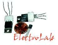
Circuit symbol of a diode  T he p- and n-type semiconductors are used in creating a
semiconductor diode. Actually, a diode is prepared by doping a semiconductor melt
predominantly with p-type impurity in one part and with n-type in another part. As a
result, the p-region contains majority of holes and the n-region contains majority of
electrons. These holes and electrons tend to diffuse over their junction and hence create
a barrier region with a very high resistance, thus preventing the further diffusion on
holes and electrons in the absence of P.D.
T he p- and n-type semiconductors are used in creating a
semiconductor diode. Actually, a diode is prepared by doping a semiconductor melt
predominantly with p-type impurity in one part and with n-type in another part. As a
result, the p-region contains majority of holes and the n-region contains majority of
electrons. These holes and electrons tend to diffuse over their junction and hence create
a barrier region with a very high resistance, thus preventing the further diffusion on
holes and electrons in the absence of P.D. The function of a diode is to act as a valve, permitting the flow of current only in one direction. A semiconductor diode permits the flow of (conventional) current from p-region to the n-region and offers a large resistance from n-region to p-region. This can be explained by considering the biasing of diodes. |
Forward Biased:

The p-region of the semiconductor is connected to the positive terminal of the source and the n-region of semiconductor to the negative terminal of the source. As a result, both the holes and electrons move towards the junction of the diode from p- and n-regions respectively. Consequently, the resistance of the barrier decreases and the current flows through the diode.
. |
Hole | . |
Electron |
Reverse Biased:
 The p-region of the semiconductor is
connected to the negative terminal of the source and the n-region of semiconductor to the
positive terminal of the source. As a result, both the holes and electrons move away from
the junction of the diode from p- and n-regions respectively. Consequently, the resistance
of the barrier increases greatly and practically no current flows through the circuit.
However, a minute current may be noted due to the minority charge carriers in the
semiconductors i.e. a small number of holes in n-region and free electrons in p-region
formed due to thermal ionization.
The p-region of the semiconductor is
connected to the negative terminal of the source and the n-region of semiconductor to the
positive terminal of the source. As a result, both the holes and electrons move away from
the junction of the diode from p- and n-regions respectively. Consequently, the resistance
of the barrier increases greatly and practically no current flows through the circuit.
However, a minute current may be noted due to the minority charge carriers in the
semiconductors i.e. a small number of holes in n-region and free electrons in p-region
formed due to thermal ionization.
. |
Hole | . |
Electron |
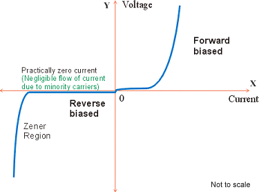
Also at highly negative potential, a phenomenon called Zener effect occurs, causing a high negative current (avalanche current) to flow.
The relation between the voltage and the electric current flowing through the diode can be graphically represented as: