


![]()
![]()
![]()
ADVANCED
Let us consider an amplifying circuit of a Bipolar Junction Transistor to completely understand its working and amplification process.
As you have learnt under BJT in the
Typessection, it is necessary to
keep the Emitter and the Base forward-biased and to keep the Base and collector
reverse-biased. The adjoining circuit explains how this is done. Let us consider the
functions of the various circuit components:
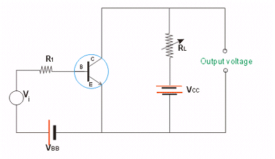
Vi:
This is the input voltage. It is usually a fluctuating, alternating voltage.
VBB:
This is a steady direct voltage. It supercedes the input voltage and helps to ensure that
the Emitter-Base combination is always forward-biased. Hence, even if the input voltage is
in the opposite direction, the resultant voltage is always in one direction.
R1: This is a small resistance that is used to control the input current.
RL: This is a variable load resistance and is generally very large. It is adjusted to obtain the desired output voltage. As this resistance has a very large value, and as it is coupled with the large resistance offered by the reverse-biased output circuit, it ensures a large output voltage.
VCC:
This is a steady, direct voltage and it helps to ensure that the output circuit is
reverse-biased.
The working of the BJT now becomes clearer in light of its amplification circuit.
The amplification process in case of a JFET or MOSFET can be easily understood from its
working and hence its circuit has not been discussed here. Moreover, the circuit of either
transistor is generally quite complicated.