
Scientific Aspects
Click to learn about the development of this transistor
The MOSFET may be considered as a much-advanced upgrade of the JFET. It has shown great promise of achieving wide commercial acceptance and is the most commonly used transistor in the highly complex electronic devices. However, MOSFET too is present in different types. We shall, for the sake of simplicity, consider the Depletion-Enhancement or simply DE-MOSFET, which is the modified version of MOSFET and is the most suitable one.
Construction:
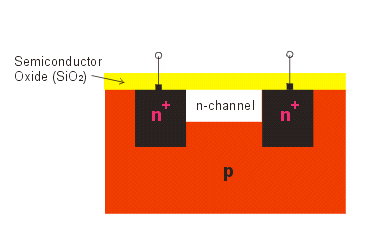
Consider a MOSFET shown in the adjoining diagram. It consists of a p-type semiconductor (shown in red) with two n-regions (shown in black) that are embedded into it by special techniques. These n-regions contain extremely high number of charge-carriers (electrons) and so are represented as n+. This combination is then covered over by a layer of the semiconductor's oxide. In between the two n+ regions, is another channel of n-type semiconductor (shown in white), containing less number of charge carriers than the n+ regions
Working:
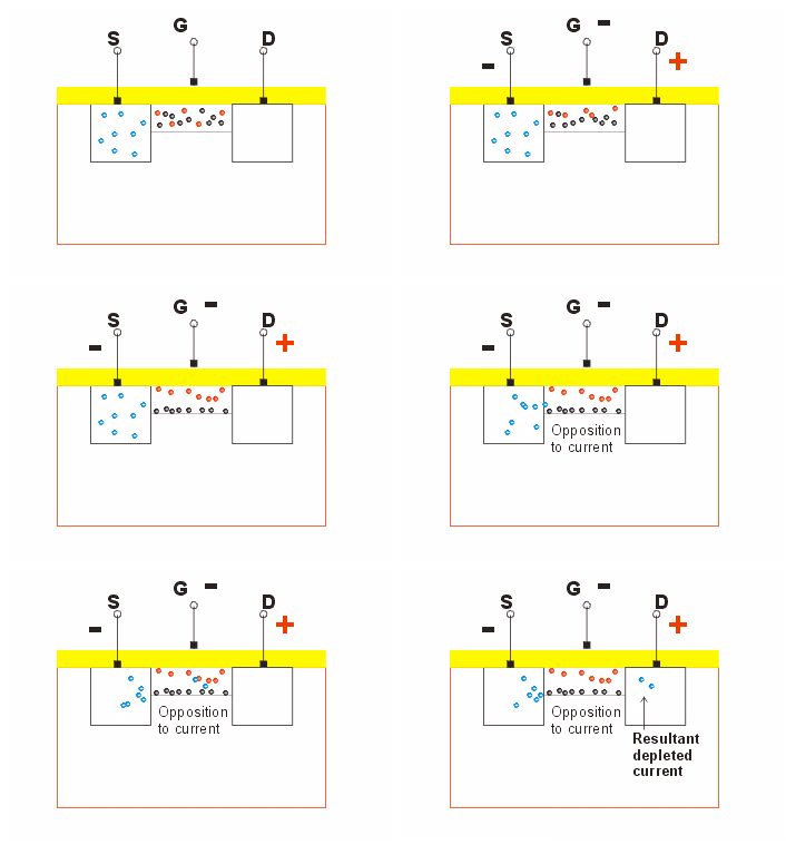
When a negative charge is applied above the layer of oxide, the n-channel attracts most available positive charges (holes) towards itself (since opposite charges attract). Thus the flow of electric current, which is actually the flow of negatively charged electrons is reduced due to the presence of the opposite positive charge. This is called as Depletion of current.
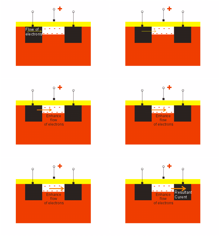
On the other hand, when a positive charge is applied above the layer of oxide, the n-channel attracts more electrons towards itself. Thus the flow of current, which is nothing but the flow of electrons, is enhanced by these surplus electrons.
Hence the name, Depletion-Enhancement MOSFET.
Here, the n+ region from where the electron current enters is called as the Source. The other n+ region from where they leave is the Drain. The charge above the oxide layer is called as Gate. Thus, just as in case of a tap, the flow fom the Source to the Drain is controlled by the Gate.
The same explanations are valid for p-channel MOSFET. However, the electrons will be replaced by holes and vice versa, and the charges will be reversed.


|
Development-Scientific |
Development-Scientific |
|
Development-Scientific |
Development-Scientific |
T
he MOSFET may be considered as a much-advanced upgrade of the JFET. It has shown great promise of achieving wide commercial acceptance and is the most commonly used transistor in the highly complex electronic devices. However, MOSFET too is present in different types. We shall, for the sake of simplicity, consider the Depletion-Enhancement or simply DE-MOSFET, which is the modified version of MOSFET and is the most suitable one.
Construction:
Let us consider an n-channel DE-MOSFET. It consists of a lightly doped p-substrate into which are etched two highly doped n-regions. These two regions are so highly doped that they are represented as n+. The oxide of the semiconductor (e.g. SiO2) then layers this combination. The two n
Working:
The voltage that is to be amplified is applied between the Drain and the Source and is called as the Drain-Source voltage (V
When VGS is made negative, the gate terminal G acquires a negative potential. Consequently, there occurs an induction of charges through the semiconductor oxide, as shown. As a result, the positive charges that are present in the n-channel get concentrated towards the gate terminal, thus reducing the flow of electrons from the Source to the Drain. This reduction of electric current is called as Depletion.
Converse effect is observed when VGS is made positive. The gate terminal G now acquires a positive potential. Once again, an inductive effect is observed and this time, the negative charges that are available are concentrated towards the oxide layer. Thus, they help in facilitating the flow of current between the Source and Drain. This effect is called as Enhancement.
Thus the oxide layer prevents the direct contact between the gate and the n-channel, thus preventing the flow of current between them. Also, the n-channel plays an important role by providing adequate positive and negative charges during induction.
The same explanation is valid for p-channel MOSFET. But the regions, charges and the voltages will have to be reversed.


|
Development-Scientific |
Development-Scientific |
|
Development-Scientific |
Development-Scientific |
|
Introduction to Semiconductors
This topic will introduce you to the concept of semiconductors which are an integral part in the making of transistors. |
|
Semiconductor Diodes
The prerequisite information on diodes that later went on to give the birth to the semiconductor triode - otherwise known as the transistor. |
|
Semiconductor Triodes
Another name for the transistor... |
|
Types of Transistors
Learn the various types of transistors and how they function. |
|
Amplification
This is the basic function of the transistor - and the most important one! |
|
Switches
Next to amplification, this is the most common function of transistors. |
|
Comparisions
Learn the analogies and the differences between the older vacuum tube triodes and the slicker new transistors. |
|
Integrated circuits
These are the most common applications of transistors and go a long way in building powerful microprocessors and appliances. Learn the role that transistors play in them. |
|
Microprocessors
These are the real brains of most electronic appliances around us. Explore the vital role played by their grey cells - transistors. |
|
Appliances affected
Realize the full potential of these transistors through the various appliances they revolutionized, right from your digital watch to this PC. |
|
The pre- and post-transistor world
To understand the impact of the transistor in its entirety, perceive what the world was before, and what it is after 1947 - when the transistor was invented. |
|
Future trends
Revolution is an unending process. Take a sneak preview of where the transistors of the future are headed. |
|
History
Understanding of the transistor becomes clearer when learnt in context of its evolutionary journey. Here, we have presented the most important landmarks in its journey of almost a century. |
|
Build the transistor
Theoretical knowledge weighs nothing unless put to practice. Learn how the different types of transistors are built and build some on your own! |
|
Learn the circuits
Learn how the actual amplification and switching takes place by building your own circuits and watching the current flow. |
|
Drive-the-circuit
If you have the necessary stuff in your head, come and test drive a BJT amplification circuit! But watch out for the speed bumps along the way! |
|
Message Boards
Leave your own messages and discuss different topics with fellow surfers. |
|
Ask-a-mentor
Nobody's perfect...we are no exception. But we certainly try to be perfect. If you have any questions about transistors that were not answered in this site, ask our mentors... |
|
Related links
Related links on the web about transistors. |
|
Learners' Center
Discuss your views with other users of this site. There are topics like Message Board, Translate-the-site and Simplify-the-site! |
|
Quizzes
These are quizzes to rack your grey cells. If you think that you have surfed this site entirely, solve these! They include Multiple choice questions and Scrambled words to solve! |
|
Learn in a Flash
These are our step-by-step interactive tutorials to brief you up about the world of transistors. |
|
Advanced Section
This section includes an in-detail explanation on this topic. For you to understand the Advanced section, you should have a basic knowledge of the fundamentals involved. To learn more, please select the section called Prerequisites from the bottom of the page. |
|
Basic Section
Return to the Basic section. |
|
Prerequisites
This section is meant to explain the fundamentals involved in the knowledgae of transistors! This page opens in new window |
|
Site Map
This page will show the map of ...trailing the Transistor for your easier navigation. |
|
Citations and Copyrights
A list of our sources and also copyright notices of material used in making this site. This page opens in new window |
|
Development of PCT
Learn the development of Point Contact Transistor. |
|
Development of BJT
Learn the development of Bipolar Junction Transistor Transistor. |
|
Development of JFET
Learn the development of Junction Field Effect Transistor. |
|
Development of MOSFET
Learn the development of Metal Oxide Semiconductor Field Effect Transistor. |
|
Scientific Aspects of PCT
Learn the scientific aspects of Point Contact Transistor. |
|
Scientific Aspects of BJT
Learn the scientific aspects of Bipolar Junction Transistor. |
|
Scientific Aspects of JFET
Learn the scientific aspects of Junction Field Effect Transistor. |
|
Scientific Aspects of MOSFET
Learn the scientific aspects of Metal Oxide Semiconductor Field Effect Transistor. |
|
You are currently here:
Transistors -- Types -- Scientific Aspects of MOSFET |
|
|